Products
Technology
Questions & Answers
These question are mostly related to the Flexibilis Redundant Switch (FRS). Since FRS is one configuration of the Flexibilis Ethernet Switch (FES), many of the answers are also true for FES.
To search for a specific question, in most browsers you can press CTRL+F and then type in a word to search. The questions are sorted in the following categories:
- General Questions
- Performance Questions
- Interface Questions
- IEEE 1588 Questions
- Evaluation Questions
General Questions
- What are the supported FPGA models?
Altera Cyclone IV, Altera Cyclone V and Cyclone V SoC are the preferred FPGA models. However, FRS is vendor independent. For other solutions, please contact us. - What is the advantage of Layer-2 redundancy compared to Layer-3?
The Layer 2 redundancy protocols HSR and PRP are much easier from maintenance and service point of view because single nodes can be replaced or unplugged on the fly without affecting the other nodes. In L3 network unplugging a node starts a rerouting process, during which frames are lost.Also, in L3 network the IP address of each node must be configured. Each L2 node has always a unique address.
- Is it possible to use Rapid Spanning Tree Protocol (RSTP) with FRS?
Yes it is. FRS supports the ports states (disabled, learning, forwarding) required from the switch core. The spanning tree protocol implementation however is not a feature of FRS; the RSTP protocol has to be implemented with software. - What size is the frame buffer for the demo environment?
640 kbits, common for all ports. - Is the depth of the frame buffer configurable?
The size of the buffer memory is fixed and depends on the port count:
3 port, 4 priorities = 384 kbit
4 port, 4 priorities = 512 kbit
5 port, 4 priorities = 640 kbit
6 port, 4 priorities = 768 kbit
7 port, 4 priorities = 896 kbit
8 port, 4 priorities = 1024 kbit
3 port, 8 priorities = 768 kbit
4 port, 8 priorities = 1024 kbit
5 port, 8 priorities = 1280 kbit
6 port, 8 priorities = 1536 kbit
7 port, 8 priorities = 1792 kbit
8 port, 8 priorities = 2048 kbit - Can you provide some example figures on FPGA resource usage for a four (plus the management) port implementation of FRS-Core?
Here’s as an example report for 5-port FRS with FRTC:
Fitter Status : Successful - Tue Feb 23 17:23:33 2016

Quartus Prime Version : 15.1.0 Build 185 10/21/2015 SJ Standard Edition

Revision Name : fes_and_frtc_with_mdio

Top-level Entity Name : fes_and_frtc_with_mdio

Family : Cyclone V

Device : 5CEFA5F23I7

Timing Models : Final

Logic utilization (in ALMs) : 18,277 / 29,080 ( 63 % )

Total registers : 38713

Total pins : 154 / 240 ( 64 % )

Total virtual pins : 0

Total block memory bits : 1,483,801 / 4,567,040 ( 32 % )

Total RAM Blocks : 181 / 446 ( 41 % )

Total DSP Blocks : 20 / 150 ( 13 % )

Total HSSI RX PCSs : 0

Total HSSI PMA RX Deserializers : 0

Total HSSI TX PCSs : 0

Total HSSI PMA TX Serializers : 0

Total PLLs : 0 / 6 ( 0 % )

Total DLLs : 0 / 4 ( 0 % )
- Can the time-out value be set for 1000Base Ethernet and 100Base Ethernet?
Both the MAC address life time (ProxyNodeTableForgetTime in HSR) and the HSR/PRP EntryForgetTime are user configurable. See the register map in the Manual, chapter 5. - How many multicast addresses can be filtered?
The MAC address filter has 16 entries per port, see Inbound Policy in chapter 4.1.6 of the Manual. This number includes multicast addresses. Addresses can be aggregated. There is also an optional feature called Static MAC Table that supports filtering of up to 16,384 addresses. It is described in Manual chapter 4.1.11. - There are many versions of IEC 62439-3. Each one is with some different formats. Which version of IEC 62439-3 does FRS support?
FRS supports the latest version of the standard. Both PRP (Clause 4) and HSR (Clause 5) are supported. - Will the bitstream file merge HSR/PRP in single code so that users could change function easily by themselves?
Yes, FRS supports both HSR and PRP, the mode can be changed between HSR and PRP using the register interface. At Altera evaluation board (our demo setup) it can be selected with a DIP switch whether the ports are in HSR or PRP mode. - Can you show the block diagram?
The block diagram of FRS can be found in the Manual. The block diagram of the Cyclone V reference design is presented in the figure below: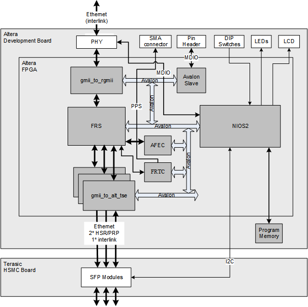
- Does FRS include a Microcontroller?
FRS does not include a Microcontroller. An external (to FRS) controller/CPU has to be connected to FRS. The controller can be a soft core processor inside the FPGA, or it can be a separate chip next to the FPGA. A microcontroller is needed to:– Configure the functionality of FRS
– Implement IEEE1588v2 ordinary/boundary clock
– Implement HSR/PRP supervision protocol
– Implement RSTP
– Implement other OSI layer3 and above protocols - What flash size should we use?
There is information on the selection of Flash type (and FPGA configuration method) in the following Altera document:
http://www.altera.com/literature/hb/cyclone-iv/cyiv-51008.pdf. You should choose the Flash size based on the FPGA size you have, if you are using a separate Flash device for the FPGA configuration. Note that it is also possible to configure the FPGA with your CPU. In that case you do not need to have a separate Flash device for the FPGA, which saves you the cost of the Flash chip. - What is the IP bitstream code size?
The size of the configuration bitstream depends on the selected FPGA, because it contains configuration for the whole FPGA device. The size of the configuration bitstream for example for EP4CGX50 is 24,500,000 bits, see http://www.altera.com/literature/hb/cyclone-iv/cyiv-51008.pdf, Table 8–2.This means that without compression, the configuration bitstream will fit to EPCS64 whose size is 67,108,864 bits (see Table 1 in http://www.altera.com/literature/hb/cfg/cyc_c51014.pdf). With Configuration Data Decompression (see page 8-2 in http://www.altera.com/literature/hb/cyclone-iv/cyiv-51008.pdf) the configuration data fits to EPCS16 as its size is 16,777,216 bits and the configuration bitstream will compress (at least) to 24,500,000*0.65 = 15,925,000 bits.
- Do you have a Linux driver for Gigabit Ethernet?
In addition to FRS you’ll need an Ethernet controller to be able to send/receive Ethernet frames using your CPU. The Ethernet controller can be integrated into the CPU, it can be a separate chip, or it can be an IP block at the FPGA. Our own Ethernet controller IP block is called AFEC and we have Linux drivers for it. FRS has Linux drivers available in the reference design packet. - What else is needed in addition to FRS?
This of course depends on your application. In most of the cases a CPU is needed, to be able to run supervision protocols and IEEE 1588 PTP protocol stacks. The CPU can be either a softcore processor (NIOS II) on the FPGA, a hardcoded processor on the same chip with the FPGA (SoC), or it can be a separate chip. An Ethernet controller is needed for the CPU to be able to send/receive frames. The Ethernet controller can be integrated into the CPU, or it can be on the FPGA chip. Both options are presented in the figure. Note that IEEE 1588 PTP support is not required in the Ethernet controller, as all the timestamping functionality is integrated in FRS. You can run your own application(s) on the same processor, or on another processor. In the picture the components that can be provided by Flexibilis are marked with Flexibilis logo.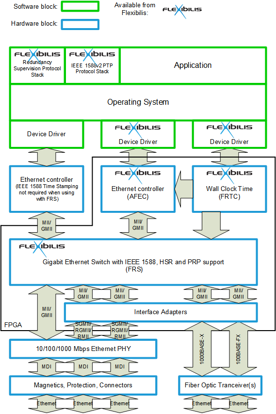
- Which features are implemented in HW, which ones in SW?
Please see the table.Feature: Pure HW Both SW and HW Notes General Switch Functionality: Forwarding Ethernet Frames x Address learning x Address aging x Error checking (CRC) x RSTP x RSTP SW implementation not available from Flexibilis HSR & PRP Functionality: Duplicate generation x Duplicate removal x Insertion & removal of HSR & PRP tag x Redundancy Supervision x 1588v2PTP Functionality: End-to-End Transparent Clock x Peer-to-Peer Transparent Clock x SW calculates the link delay. HW does the real time corrections. Ordinary Clock x SW runs the PTP protocol stack. HW timestamps frames. Boundary Clock x SW runs the PTP protocol stack. HW timestamps frames. - How can we configure FRS to function as a QuadBox?
A QuadBox is formed by:
1. Having two FRS instances
2. Configuring the both FRS instances to have an HSR interlink port (HSR-HSR RedBox mode)
3. Connecting the HSR interlink ports (of the two FRS instances) to each otherThere isn’t any special QuadBox bit in FRS registers.
- How to use and configure the IPO?
Please see this document for Inbound Policy (IPO) configurations: FRS_IPO_Configuration.pdf. The document gives examples on how to use the IPO configurations in FRS IP with PTP
and HSR/PRP protocols. Before looking at this document, please read the Inbound Policy section from the Manual. - If I want to start using some of the additional features, how should I proceed?
The first requirement is that your design is using FES (or FRS) core version 3.0 or newer. Older FES/FRS version do not support additional features, so if you are using an older version you must first update your design. Have a look at the “FRS to FES Migration” documentation for more information about the migration from 2.9.4 to 3.0 version.Second step is to enable the required features for evaluation using the OCP license. The migration documentation defines how additional features are enabled and taken into evaluation. When you have evaluated the functionalities and want to enable the full use of the functionalities (not OCP), contact Flexibilis for licensing information.
- Can I add some of the additional features into my design in the future? Does the FES core change if I add some additional features?
The most important requirement is that your design is using FES (or FRS) version 3.0 or newer, since older version do not support additional features. If your design is using correct version of FES/FRS it is fairly simple to include some or all of the additional features into your design also in the future. However, it should be noted that some additional functionalities will increase the resource consumption significantly. It is possible to evaluate the additional features and their resource consumption even without a full license. - Can some of the additional functionalities be added to 2.9.4 version of the FRS?
No, unfortunately additional features are only available for FES/FRS version 3.0 and newer.Performance Questions
- What do latency, store-and-forward and cut-through mean in practice?
Cut-through operation means that a switch starts to forward an incoming frame before it has fully received it. A store-and-forward switch always receives the whole frame before forwarding it. Cut-through operation minimizes the forwarding delay (latency) but does not fully conform to IEEE standard 802.1D “Media Access (MAC) Bridges” because in cut-through mode it is not possible to check the CRC of the frame which causes broken frames to be forwarded by the switch. By using cut-through operation it is possible to minimize the minimum latency, but it does not affect the worst-case latency, which is typically more important. Other methods for minimizing latency (especially worst-case latency) are usage of proper prioritization mechanisms and increasing of the line speed. - How about latency and performance data?
The forwarding performance is one gigabit per port, wire-speed and full-duplex, all the ports at the same time. The forwarding latency of FRS (measured according to RFC 2544) is presented in the figure: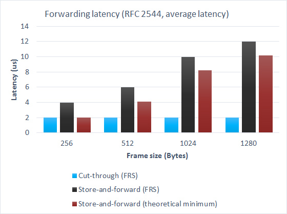
Interface Questions
- CPU Interface and its internal register description?
The internal registers of FRS are presented in the Manual, in chapter 5. The configuration interface of FRS is Avalon, but the FRS reference design includes MDIO Slave component, which enables accesses from the MDIO to the Avalon. In addition the reference design provides support for XR7 Firmware Configurator, which may be used to control FRS operation over Ethernet. The XR7 Firmware Configurator is running on NIOS. By having bridges from a technology to another it is basically possible to access FRS registers using any technology (I2C, SPI, PCIe, …). - FPGA pinout and pin description?
The FPGA pinout is not fixed by Flexibilis. The user can connect the I/O of FRS to the I/O of the FPGA or to other blocks at the FPGA as they wish. - Does FRS support SGMII/1000BASE-X interface?
FRS has MII/GMII interfaces natively. With separate interface adapters (inside FPGA but outside FRS) we are able to support also RMII, RGMII, SGMII, 1000BASE-X and 100BASE-FX.For example, by using 1000Base-X adapters gigabit SFP fiber optic modules can be connected directly to the FPGA. - What are the signals tx_time_word(95:0) and rx_time_word(95:0) for?
An (external to FRS) real-time clock is connected into these signals. The clock time information is needed by the IEEE 1588 PTP functionality of FRS. The real-time clock can be left out, if IEEE 1588 functionality is not needed. The Flexibilis real-time clock IP is called FRTC. - Can you provide FRS for our target board/chip/pinout?
Flexibilis provides a bitstream for selected demo boards, currently for Altera Cyclone IV and Cyclone V evaluation boards. In addition to that Flexibilis provides FRS in encrypted VHDL form so that our customers can themselves compile FRS for their target chip and for their own pinout. The customers are also able to include other blocks to their compilation. Flexibilis provides also a reference design for Quartus Prime tool and selected Altera evaluation boards. - How should I set the PORT_STATE speed selection and HW mode with different adapters?
FRS port speed selection (PORT_STATE bits 8-9) and HW mode (bits 4-5) must be selected to match the interface type used. The following table shows the possible interface adapters and related speed and HW mode selections.Adapter and Speed FRS Port Mode 10 Mbps, MII 100 Mbps, MII 1000 Mbps, GMII 100BASE-FX x 1000BASE-X x SGMII, 10 Mbps x SGMII, 100 Mbps x SGMII, 1000 Mbps x RGMII, 10 Mbps x RGMII, 100 Mbps x RGMII, 1000 Mbps x RMII, 10 Mbps x RMII, 100Mbps x
The 1000Base-X and 100Base-FX adapters support only a single speed, so the interface speed of FRS can be fixed to that. RGMII and SGMII support different speeds, so the user should read the result of the autonegotiation from the registers of the adapter (or the PHY) and configure that negotiated speed to FRS. When interfacing to a PHY device with GMII/MII or RGMII interface the speed and the HW mode must be set according to the PHY auto-negotiation results that can be read from the registers of the PHY. In case of device internal Ethernet interface, for example between FRS and an on-board CPU, the interface speed can be fixed to a desired setting. Note that when the interface speed setting is a result of an autonegotiation process it has to be constantly polled by the software for changes. Please note also that some adapters support also automatic speed selection signals towards FRS.
IEEE 1588 Questions
- Does FRS support IEEE 1588 ordinary clock?
FRS does not implement a full IEEE 1588 ordinary clock. However, in its CPU port FRS implements functionality that timestamps PTP Event messages and modifies PTP Sync messages. Customers who wish to run IEEE 1588 ordinary clock functionality at their CPU and who do not have IEEE 1588 support in their Ethernet MAC can use this hardware timestamping & modification functionality of FRS to greatly increase the accuracy of their IEEE 1588 ordinary clock implementation. Information on Flexibilis’ IEEE 1588 PTP protocol stack can be found at https://www.flexibilis.com/products/xr7-ptp/. Users of FRS can use the stack provided by Flexibilis, or implement their own ordinary clock. - Does FRS support hybrid clock (that combines a transparent clock and an ordinary clock)?
FRS implements a transparent clock, but it does not implement IEEE 1588 ordinary clock. Information on Flexibilis’ IEEE 1588 PTP protocol stack that includes an ordinary clock can be found at https://www.flexibilis.com/products/xr7-ptp/. - Does FRS support one step clock / two-step clock? Is there a mechanism to select one-step/two-step clock?
FRS implements 1-step transparent clock, but no 2-step. Note that 1-step clock is fully compatible with 2-step clock, i.e. there can be 1-step and 2-step clocks in the same network and everything works as it should. - Does FRS support peer-to-peer transparent clock?
Peer-to-peer (P2P) transparent clock is supported with some help from the IEEE 1588v2 protocol stack running on the CPU: In the P2P transparent clock case SYNC messages are forwarded by the FRS, with minimal delay and without software intervention. Link delay calculations are made by the CPU and the CPU writes the result of the link delay calculation to FRS register. - Does FRS support end-to-end transparent clock?
Yes, FRS implements an end-to-end transparent clock with pure hardware. - PTP transparent clock is included in the FRS core, so why are there time interfaces? Shouldn’t it be sufficient to use the fes_default_clock module output as in the reference design?
The PTP transparent clock in FRS modifies the PTP messages as they pass through the device. However, FRS requires time information from outside and Time Interface is used for this purpose. The fes_default_clock found in the reference design is sufficient for many cases; it is not adjustable, but adjustable clock time is not necessary for PTP transparent clock functionality. If adjustable clock (adjustable time and/or speed) is needed use FRTC (Flexibilis Real-Time Clock) instead of fes_default_clock. - Can FRS run both of IEEE 1588 boundary clock and transparent clock at the same FPGA simultaneously?
It is possible to have a boundary clock and a transparent clock at the same time. Transparent clock is a feature of FRS, and boundary clock is a feature of the 1588 PTP protocol stack running on the CPU, so the boundary clock is technically not on the FPGA. - What is the accuracy of the IEEE 1588 performance of FRS?
Nanosecond class accuracy has been achieved with FRS by using gigabit fiber optic links. In practice, FRS is not the component that limits the accuracy that can be achieved, but rather the unpredictable delays of the PHY chips, the wander of the oscillator, and so on. Sub-microsecond accuracy is typical with normal low-cost components and sync message interval of one second. Note that MEMS type oscillators are not recommended because of their sudden frequency jumps. - As IEEE1588 frames are sent to CPU, is the time that FPGA triggered attached to those frames and sent to CPU?
Yes, FRS inserts the time information to the frame when the feature is enabled. It is also possible to read the information from the registers of FRS. - Are there any internal registers for IEEE 1588?
For peer-to-peer transparent clock there are registers for the link delay. Then there are registers for compensating delays caused by interface adapters, PHYsical layer chips and other hardware components. For end-to-end transparent clock there is a setting whether the IEEE1588v2 protocol is run over Layer2 (Ethernet) or Layer3 (IP). Then for ordinary/boundary clock there are registers for controlling the timestamping and modifying of the frames. - What are the functions for IEEE 1588 inside the FPGA core?
FRS implements IEEE1588v2 transparent end-to-end clock functionality with pure FPGA. For IEEE1588v2 transparent peer-to-peer clock and ordinary/boundary clock FRS has support functionality (but no full implementation), so that IEEE1588v2 support can be implemented with best possible performance. - If we use your HSR/PRP and IEEE1588 solution in the system, do we need to have real time clock in the system?
IEEE1588 uses wall clock time that it synchronizes in all devices in the network. This wall clock time is normally implemented as an IP block in FPGA. We provide an implementation as a part of the FRS reference design.IEEE1588 Power Profile (for example) guarantees that all devices in the network are synchronized with 1us accuracy after 30s from device boot. Normally there is at least one IEEE1588 clock master in the network that is synchronized to some external clock, for example GPS, atomic clock or perhaps only to RTC (when it is not required that network is synchronized to UTC time: it is enough that all devices in the network have the same time).
Need for external RTC depends a little on the customer application. In the usual case, it is enough to use only IEEE1588 to synchronize slave clocks and at least one of the devices need to be able to act as a clock master.
- The IEEE 1588 stack takes into account the delay of the synchronization frames through the network, and was designed assuming that there is only one way. However, HSR/PRP redundancy implies the existence of two paths that synchronization frames can reach the node and one of the two redundant frames is eliminated. Therefore, the IEEE 1588 stack has problems on the one hand to calculate the delay for each way, and it doesn’t know which of the two paths must be considered for synchronization.
The question is twofold:
– Do you apply the discarding algorithm to IEEE 1588 frames?
– Is there any indication for IEEE 1588 stack on the origin of the frame, ie: if the frame comes from the branch one or two?
We let all the IEEE 1588 frames go to the CPU. We use the mirroring functionality of our IPO filter (see Table 9. “Inbound Policy Registers” in the Manual) to mirror all the IEEE 1588 frames to the CPU port thus disabling the HSR/PRP duplicate discard functionality for IEEE 1588 frames. See also FRS_IPO_Configuration.pdfThe bits in the Management trailer (see Chapter 4.1.7 “Management Trailer” in FES Manual) indicate to the CPU from which (HSR/PRP) port the frame was received.
Evaluation Questions
- I downloaded the HSR/PRP reference design. I generated the Qsys system, then tried compiling, but Quartus threw an error. Why?
You need to download the IP core too. It can be downloaded from Downloads page.Unzip the reference design packet (FESHA00E00-FBIT.zip) somewhere at your computer. Create a folder named encrypted_ip in it, in the main directory (first level, in the same folder with cyclone4GXdevkit_eva, cyclone5GXdevkit_eva and doc).
Then unzip also the IP Core packet. From there you can find a directory named core. Copy the contents of this directory to the encrypted_ip folder you created. Now you should be able to compile the design.
If it still doesn’t work after this, try setting the license files. In Quartus Prime, this can be done at Tools -> License Setup.
- Can I evaluate shaper or policer functionality on the reference board or on my own HW?
Yes you can. The additional features of FRS like policers and shapers are provided with an OCP license with the FRS IP core. OCP license allows generation of a time limited .SOF file, which can be used to evaluate the design. To test an additional feature the user must enable the required functionality from the QSYS or using the FRS generics directly. In addition it is necessary to include the related .vhd file and .ocp file to your project as well as introduce the OCP license file to the Quartus. It is recommended to read the “FRS to FES Migration” document and especially chapter 5 “Testing additional features using OCP”. Migration document is included in the reference design packages. - Is there any reference board available with all the additional features included?
The Cyclone V SoC FRS evaluation design for Terasic SoC board includes all the additional features.